Intel 80C186EA Manuale Utente
Navigare online o scaricare Manuale Utente per Processori Intel 80C186EA. Intel 80C186EA User's Manual Manuale Utente
- Pagina / 50
- Indice
- SEGNALIBRI
- October 1995 1
- COPYRIGHT 1
- INTEL CORPORATION, 1995 1
- Order Number: 272432-003 1
- 272432–1 1
- CONTENTS PAGE 2
- 272432–2 3
- INTRODUCTION 4
- 80C186EA CORE ARCHITECTURE 4
- Bus Interface Unit 4
- Clock Generator 4
- 80C186EA PERIPHERAL 5
- ARCHITECTURE 5
- Interrupt Control Unit 5
- Timer/Counter Unit 5
- 00H Reserved 6
- 40H Reserved 6
- 80H Reserved 6
- C0H DMA0 Src. Lo 6
- DMA Control Unit 7
- Chip-Select Unit 7
- Refresh Control Unit 7
- Power Management 7
- PACKAGE INFORMATION 9
- Pin Descriptions 9
- 80C186EA PINOUT 15
- NOTES: 272432–5 16
- NOTES: 272432–6 18
- PACKAGE THERMAL 20
- SPECIFICATIONS 20
- ELECTRICAL SPECIFICATIONS 21
- Absolute Maximum Ratings* 21
- Recommended Connections 21
- AC SPECIFICATIONS 25
- AC SPECIFICATIONS (Continued) 26
- AC TEST CONDITIONS 30
- AC TIMING WAVEFORMS 30
- 272432–12 32
- DERATING CURVES 33
- 272432–15 34
- 272432–16 35
- BUS CYCLE WAVEFORMS 36
- 272432-18 37
- 272432–19 38
- NOTES: 272432–20 39
- Figure 21. HOLD/HLDA Waveform 40
- 272432–22 41
- Figure 23. Ready Waveform 42
- 80C186EA/80C188EA EXECUTION 43
- INSTRUCTION SET SUMMARY 44
- (Continued) 45
- REVISION HISTORY 50
Sommario
*Other brands and names are the property of their respective owners.Information in this document is provided in connection with Intel products. Intel
80C186EA/80C188EA, 80L186EA/80L188EATable 2. Pin Description NomenclatureSymbol DescriptionP Power Pin (ApplyaVCCVoltage)G Ground (Connect to VSS)I In
80C186EA/80C188EA, 80L186EA/80L188EATable 3. Pin DescriptionsPin Pin Input OutputDescriptionName Type Type StatesVCCP POWER connections consist of six
80C186EA/80C188EA, 80L186EA/80L188EATable 3. Pin Descriptions (Continued)Pin Pin Input OutputDescriptionName Type Type StatesA18:16 O H(Z) These pins
80C186EA/80C188EA, 80L186EA/80L188EATable 3. Pin Descriptions (Continued)Pin Pin Input OutputDescriptionName Type Type StatesWR/QS1 O H(Z) WRite outpu
80C186EA/80C188EA, 80L186EA/80L188EATable 3. Pin Descriptions (Continued)Pin Pin Input OutputDescriptionName Type Type StatesMCS0/PEREQ I/O A(L) H(1)
80C186EA/80C188EA, 80L186EA/80L188EA80C186EA PINOUTTables 4 and 5 list the 80C186EA pin names withpackage location for the 68-pin Plastic Leaded ChipC
80C186EA/80C188EA, 80L186EA/80L188EATable 5. PLCC Package Location with Pin NamesLocation Name1 AD15 (A15)2 AD73 AD14 (A14)4 AD65 AD13 (A13)6 AD57 AD1
80C186EA/80C188EA, 80L186EA/80L188EATable 6. QFP (EIAJ) Pin Names with Package LocationAddress/Data Bus Bus Control Processor Control I/OName Location
80C186EA/80C188EA, 80L186EA/80L188EATable 7. QFP (EIAJ) Package Location with Pin NamesLocation Name Location Name Location Name Location Name1 AD15 (
80C186EA/80C188EA, 80L186EA/80L188EATable 8. SQFP Pin Functions with Package LocationAD BusAD0 1AD1 3AD2 6AD3 8AD4 12AD5 14AD6 16AD7 18AD8 (A8) 2AD9 (
80C186EA/80C188EA, 80L186EA/80L188EA80C186EA/80C188EA AND 80L186EA/80L188EA16-Bit High Integration Embedded ProcessorCONTENTS PAGEINTRODUCTIONÀÀÀÀÀÀÀÀ
80C186EA/80C188EA, 80L186EA/80L188EA272432–7Figure 7. Shrink Quad Flat Pack (SQFP) Pinout DiagramNOTES:1. XXXXXXXXD indicates the Intel FPO number.2.
80C186EA/80C188EA, 80L186EA/80L188EAELECTRICAL SPECIFICATIONSAbsolute Maximum Ratings*Storage Temperature ÀÀÀÀÀÀÀÀÀÀb65§Ctoa150§CCase Temperature unde
80C186EA/80C188EA, 80L186EA/80L188EADC SPECIFICATIONS (80C186EA/80C188EA)Symbol Parameter Min Max Units ConditionsVCCSupply Voltage 4.5 5.5 VVILInput
80C186EA/80C188EA, 80L186EA/80L188EADC SPECIFICATIONS (80L186EA/80L188EA)Symbol Parameter Min Max Units ConditionsVCCSupply Voltage 2.7 5.5 VVILInput
80C186EA/80C188EA, 80L186EA/80L188EAICCVERSUS FREQUENCY AND VOLTAGEThe current (ICC) consumption of the processor isessentially composed of two compon
80C186EA/80C188EA, 80L186EA/80L188EAAC SPECIFICATIONSAC CharacteristicsÐ80C186EA25/80C186EA20/80C186EA13Symbol Parameter Min Max Min Max Min Max Units
80C186EA/80C188EA, 80L186EA/80L188EAAC SPECIFICATIONS (Continued)AC CharacteristicsÐ80C186EA25/80C186EA20/80C186EA13Symbol Parameter Min Max Min Max M
80C186EA/80C188EA, 80L186EA/80L188EAAC SPECIFICATIONSAC CharacteristicsÐ80L186EA13/80L186EA8Symbol Parameter Min Max Min Max Units NotesINPUT CLOCK 13
80C186EA/80C188EA, 80L186EA/80L188EAAC SPECIFICATIONSAC CharacteristicsÐ80L186EA13/80L186EA8Symbol Parameter Min Max Min Max Units NotesSYNCHRONOUS IN
80C186EA/80C188EA, 80L186EA/80L188EAAC SPECIFICATIONS (Continued)Relative Timings (80C186EA25/20/13, 80L186EA13/8)Symbol Parameter Min Max Unit NotesR
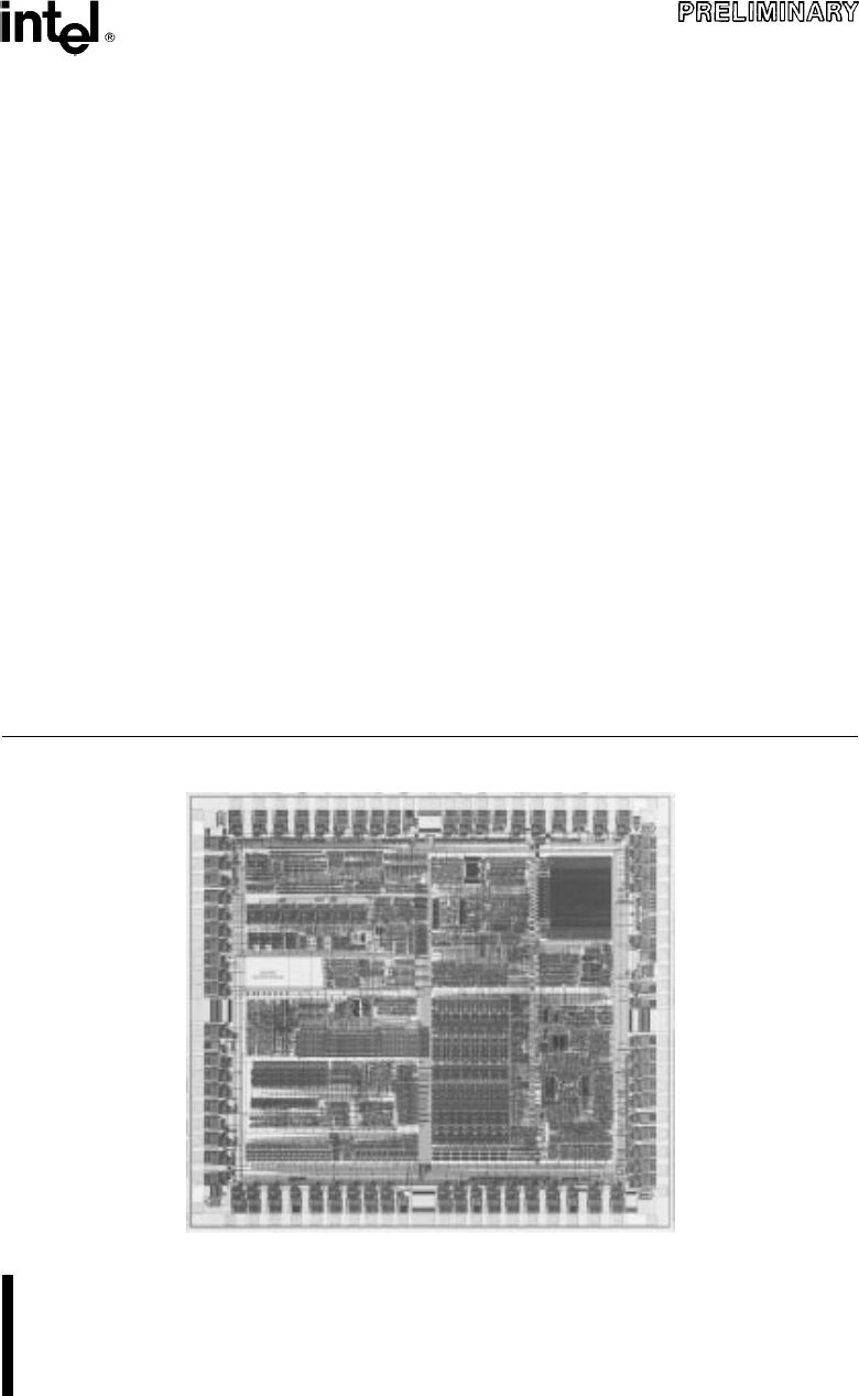
80C186EA/80C188EA, 80L186EA/80L188EANOTE:Pin names in parentheses apply to the 80C186EA/80L188EAFigure 1. 80C186EA/80C188EA Block Diagram272432–233
80C186EA/80C188EA, 80L186EA/80L188EAAC TEST CONDITIONSThe AC specifications are tested with the 50 pF loadshown in Figure 8. See the Derating Curves s
80C186EA/80C188EA, 80L186EA/80L188EA272432–10NOTE:20% VCCkFloatk80% VCCFigure 10. Output Delay and Float Waveform272432–11NOTE:RESINmeasured to CLKIN,
80C186EA/80C188EA, 80L186EA/80L188EA272432–12NOTES:1. TDXDLfor write cycle followed by read cycle.2. Pin names in parentheses apply to tthe 80C188EA.F
80C186EA/80C188EA, 80L186EA/80L188EADERATING CURVES272432–13Figure 13. Typical Output Delay VariationsVersus Load Capacitance272432–14Figure 14. Typic
80C186EA/80C188EA, 80L186EA/80L188EAFigure 15. Powerup Reset Waveforms272432–15NOTES:1. CLKOUT synchronization occurs approximately 1(/2 CLKIN periods
80C186EA/80C188EA, 80L186EA/80L188EAFigure 16. Warm Reset Waveforms272432–16NOTES:1. CLKOUT resynchronization occurs approximately 1(/2 CLKIN periods
80C186EA/80C188EA, 80L186EA/80L188EABUS CYCLE WAVEFORMSFigures 17 through 23 present the various bus cycles that are generated by the processor. What
80C186EA/80C188EA, 80L186EA/80L188EA272432-18NOTES:1. During the data phase of the bus cycle, A19/S6 is driven high for a DMA cycle.2. Pin names in pa
80C186EA/80C188EA, 80L186EA/80L188EA272432–19NOTES:1. The processor drives these pins to 0 during Idle and Powerdown Modes.2. Pin names in parentheses
80C186EA/80C188EA, 80L186EA/80L188EANOTES: 272432–201. INTA occurs one clock later in Slave Mode.2. Pin names in parentheses apply to the 80C188EA.Fig
80C186EA/80C188EA, 80L186EA/80L188EAINTRODUCTIONUnless specifically noted, all references to the80C186EA apply to the 80C188EA, 80L186EA, and80L188EA.
80C186EA/80C188EA, 80L186EA/80L188EA272432–21NOTE:1. Pin names in parentheses apply to the 80C188EA.Figure 21. HOLD/HLDA Waveform4040
80C186EA/80C188EA, 80L186EA/80L188EA272432–22NOTE:1. Pin names in parentheses apply to the 80C188EA.Figure 22. DRAM Refresh Cycle During Hold Acknowle
80C186EA/80C188EA, 80L186EA/80L188EA272432–23NOTES:1. Generalized diagram for READ or WRITE.2. ARDY low by either edge causes a wait state. Only risin
80C186EA/80C188EA, 80L186EA/80L188EA80C186EA/80C188EA EXECUTIONTIMINGSA determination of program exeuction timing mustconsider the bus cycles necessar
80C186EA/80C188EA, 80L186EA/80L188EAINSTRUCTION SET SUMMARYFunction Format80C186EA 80C188EACommentsClock ClockCycles CyclesDATA TRANSFERMOVeMove:Regis
80C186EA/80C188EA, 80L186EA/80L188EAINSTRUCTION SET SUMMARY (Continued)Function Format80C186EA 80C188EACommentsClock ClockCycles CyclesDATA TRANSFER (
80C186EA/80C188EA, 80L186EA/80L188EAINSTRUCTION SET SUMMARY (Continued)Function Format80C186EA 80C188EACommentsClock ClockCycles CyclesARITHMETIC (Con
80C186EA/80C188EA, 80L186EA/80L188EAINSTRUCTION SET SUMMARY (Continued)Function Format80C186EA 80C188EACommentsClock ClockCycles CyclesLOGIC (Continue
80C186EA/80C188EA, 80L186EA/80L188EAINSTRUCTION SET SUMMARY (Continued)Function Format80C186EA 80C188EACommentsClock ClockCycles CyclesCONTROL TRANSFE
80C186EA/80C188EA, 80L186EA/80L188EAINSTRUCTION SET SUMMARY (Continued)Function Format80C186EA 80C188EACommentsClock ClockCycles CyclesPROCESSOR CONTR
80C186EA/80C188EA, 80L186EA/80L188EA272432–3(A) Crystal ConnectionNOTE:The L1C1network is only required when using a third-overtone crystal.272432–4(B
80C186EA/80C188EA, 80L186EA/80L188EAREVISION HISTORYIntel 80C186EA/80L186EA devices are marked witha 9-character alphanumeric Intel FPO number un-dern
80C186EA/80C188EA, 80L186EA/80L188EAPCBFunctionOffset00H Reserved02H Reserved04H Reserved06H Reserved08H Reserved0AH Reserved0CH Reserved0EH Reserved1
80C186EA/80C188EA, 80L186EA/80L188EAPCBFunctionOffset20H Interrupt Vector22H Specific EOI24H Reserved26H Reserved28H Interrupt Mask2AH Priority Mask2C
80C186EA/80C188EA, 80L186EA/80L188EA80C187 Interface (80C186EA Only)The 80C187 Numerics Coprocessor may be used toextend the 80C186EA instruction set
80C186EA/80C188EA, 80L186EA/80L188EAPACKAGE INFORMATIONThis section describes the pins, pinouts, and thermalcharacteristics for the 80C186EA in the Pl
Prodotti e manuali riguardandi Processori Intel 80C186EA
 (30 pagine)
(806 pagine)
(56 pagine)
(124 pagine)
(120 pagine)
(116 pagine)
(405 pagine)
(52 pagine)
(17 pagine)
(636 pagine)
(39 pagine)
(24 pagine)
(36 pagine)
(56 pagine)
(36 pagine)
(70 pagine)
(608 pagine)
(504 pagine)
(125 pagine)
(30 pagine)
(806 pagine)
(56 pagine)
(124 pagine)
(120 pagine)
(116 pagine)
(405 pagine)
(52 pagine)
(17 pagine)
(636 pagine)
(39 pagine)
(24 pagine)
(36 pagine)
(56 pagine)
(36 pagine)
(70 pagine)
(608 pagine)
(504 pagine)
(125 pagine)
© 2020, manymanuals.it. Tutti i diritti riservati | 0.032 s |
 Manymanuals.com
 Manymanuals.de
 Manymanuals.fr
 Manymanuals.it
 Manymanuals.pl
 Manymanuals.cz
 Manymanuals.es
 Manymanuals-pt.com
Commenti su questo manuale